[RFC][VTA] Support for Cloud Devices (OpenCL-compatible)

Motivation

Cloud devices are more powerful than Edge devices, which provides higher computation capabilities for deep learning workloads. For example, for the VTA core, with Cloud devices, we have more resources to support larger GEMM cores (e.g., 32*32 or even 64*64) and device buffers, thus making it possible to boost the performance to great extent. Therefore, it is worthwhile to provide a generic framework to support cloud devices under TVM/VTA architecture.

However, it is non-trivial to extend VTA to Cloud devices. Because the original Xilinx HLS VTA core only works on Xilinx Edge FPGA devices, and Cloud devices exposes different communication models (i.e., shared memory between ARM cores and FPGA device for Edge, vs., PCIe between host and FPGA device for Cloud), and different programming models. In this work, we propose to design a unified framework that can be adapted to any OpenCL-compatible hardware accelerators, e.g., FPGA, ASICs, to seamlessly work with the TVM-VTA architecture. Meanwhile, we provide an example of OpenCL-based VTA implementation that has been tested on the Intel’s high-end FPGAs.

Proposal

We would like to extend VTA to OpenCL-compatible devices (e.g. Intel Programmable Acceleration Card). In particular, we provide a framework where any OpenCL-compatible devices can be easily integrated. The reason we choose OpenCL-compatible devices are:

  • OpenCL is generic enough to support a group of devices. For example, both Xilinx and Intel are now in transition towards OpenCL based HLS approaches.
  • Vendor-specific optimizations are built-in within their respective OpenCL SDKs (e.g., pack two 8-bit multiply-add units into 1 DSP slice), but the framework we’re providing does not limit to specific SDKs.

In addition to the generic OpenCL framework, as a first attempt for the hardware implementation, we would like to base on Intel Cloud FPGA (e.g. Intel Programmable Acceleration Card) using Intel® FPGA SDK for OpenCL, which has proven portability and scalability for both Intel® Programmable Acceleration (PAC) cards and other custom Intel-FPGA-based acceleration cards. But the overall framework is generic, meaning that any OpenCL-compatible devices can be plugged in with only little extra hardware-specific implementation.

Major works

  • Efficient communication between host and PCIe devices as PCIe transmission is costly compared to memory copy

    • To avoid frequent PCIe copies, we propose to let all middle layers of a computation graph to completely run in FPGA devices, without interleaved CPU layers. In particular, originally, residual block in Resnet run in CPU (ARM cores), which may cause copy in and out from device memory frequently. The addition of extra VTA instructions are intended to move this kind of residual block to FPGA device.
    • Do copy of uops and instructions in a batch. In particular, only do synchronization after all on-device layers are queued, or queues are overflowed.
  • Support auto-copy between layers running on different devices. We propose to add a few more IR passes:

    • annotate device types for computation graph
    • tag and propagate device types among layers
    • add copy operations (device_copy) automatically if adjacent layers are not in the same devices
  • Driver development for OpenCL-compatible devices

    • The original pynq driver could not be used as we do not have direct access to h/w registers
    • We implemented a middle layer driver for OpenCL-compatible devices
    • The layer sits on devices’ native driver stack, which implemented an interrupt based device driver
  • OpenCL hardware implementation

    • Addition of extra Load/ALU instructions, such as Load int8 to ACC buffer (to support ALU-only nodes), ALU Multiply and Left-shift, to support more continued calculations on FPGA
    • Refactored the hardware implementation code to conform to Intel® FPGA SDK for OpenCL as a sample hardware implementation

Major changes to the existing TVM/VTA framework

  • To run a workload on cloud FPGA, there is no need to launch additional service on the device side (e.g., rpc server). All the driver and runtime programs are running in the host side.

  • Change VTA runtime to support batch queue synchronization. We intend to only queue the instructions/uops when running a layer and return immediately without doing device synchronization. We only do synchronization and device run when queues are overflowed or the next layer is not on-device。

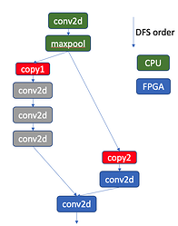
  • We have to modify the device propagation behaviour from post DFS traversal to recursive method. Originally, device type is propagated based on the post DFS traversed graph, which may not be consistent if the argument order changes. In addition, it may handle some cases wrongly, e.g., the first residual block in Resnet50. The first few layers in Resnet50 are depicted in the following figure (top to bottom is in DFS order). Basically, we want to let all the layers run on FPGA device, except the first and last few layers. In the original device propagation algorithm, based on the post DFS order, the conv2d layers in grey will be propagated with CPU device type as we encounter copy2 first, following which the three grey conv2d nodes are marked as the source device type of copy2 (i.e., CPU), which is not correct.

Limitations

  • Virtual thread is not yet supported for intelfocl devices, so all instructions are running sequentially.
  • In the first version, we require all middle layers running on the FPGA. Thus some networks whose operations in these middle layers are not supported by hardware may not be supported, as it causes a mix of CPU and FPGA operations in-between and it is hard to be annotated with correct device types automatically. This restriction can also guarantee there are no frequent device copies between layers. We may relieve this restriction in the future versions.
What do you think about this feature? @tqchen @thierry

5 Likes

also cc @vegaluis @liangfu

ping @thierry

also cc @hjiang

Thanks @zhanghaohit for your proposal. It’s quite interesting to bring VTA framework into cloud devices. It seems to be this RFC brings a quite large topic. I’ve read through the proposed change, and still unclear about:

  • OpenCL requires multi-core parallelism, and we don’t have multi-core support in VTA for now. (The topic for bringing scalability to VTA has been discussed at [VTA] Scalability for data center FPGAs )
  • How to reuse current VTA hardware to communicate with TVM runtime through PCI-e interface?

As a side note, Xilinx HLS are quite different from Intel FPGA OpenCL in my observation. I think a more easy (and efficient) workaround is to reuse Chisel VTA for the PCI-e based FPGA, and implement PCI-e based driver for DMA. @vegaluis would have more experience on this.

See also:

1 Like

Hi liangfu,

Thanks for your reply!

OpenCL requires multi-core parallelism, and we don’t have multi-core support in VTA for now.

Could you explain a bit more on this multi-core parallelism requirement of OpenCL? We intend to implement the proposed VTA core using single-work-item OpenCL kernels.

How to reuse current VTA hardware to communicate with TVM runtime through PCI-e interface?

A thin middle-layer driver is proposed to facilitate the communication between TVM runtime and the accelerator through PCIe.

Thanks!

Hi zhanghaohit,

thanks for this proposal, it is a very intersting topic, this proposal seems like be a very big change, but some parts of this proposal i am not quite understand and need your help for clarify,

first about the motivation part, this topic mentioned

#1 about “cloud device may use PCIE instead of memory share”, that make sense, but seems like a new driver with pcie support would can fix and no need such big change,

#2 about “different programming models”, could you help to give more detailed information about this part? do we have any plan to address scalibility issue for cloud fpga performance concern?

based on current information of motivation, it is little confused why we need to do this big change.

for “proposal” , this part mentioned “framework where any OpenCL-compatible devices can be easily integrated” and “Vendor-specific optimizations are built-in … SDK”, but “does not limit to specific SDK”, seems like the goal is to create a cross platform framework, this idea really awsome, but this 2 part “any OpenCL-compatible devices” and “vendor-specific optimization” are conflict, could you give more detail about what the plan here to balance this 2 parts and how to reduce related complexity to minus developer efforts?

for “major work”, about “To avoid frequent PCIe copies” “we propose to let all middle layers of a computation graph to completely run in FPGA devices”, about this part, I have couple questions first does that means this proposal would put all params data(input data, weights, bias) into FPGA sram one time? in such case if the model params size is bigger then FPGA capability how to handle such issue?

second, the data transfer may cause big latency, could I know do we have any solution to hiding the memory latency?

third, even with PCIE device, DMA should still work, could I know some detail about which “PCIe transmission is costly”?

#4 about “auto-copy between layers” seems like this is talking about inter-operator parallel, as I know tvm currently not analysis and do inter-operator parallel yet, do this proposal plan to add such support to tvm?

for “Major changes” , about “there is no need to launch additional service”(e.g., rpc server), this is a existing feature related deploy, after build network moodle, vta can running locally with any language (c++/python etc), here is a deploy example https://github.com/apache/incubator-tvm-vta/pull/5 ,

about “Change VTA runtime to support batch queue synchronization”, seems like this is current VTA logic, could I know some detail about the different between existing logic and this new synchronization logic?

about “DFS traversal”, as I know tvm seems like do network node compute sequentially instead of DFS, could I know what does this “DFS traversal” means?

about “except first layer and last layer (in FPGA)”, currently lot solution include vta(fist conv) do this, but there are also some solution offloaded all conv include #1 layer into FPGA,could I know what is the concern for putting first/last layer in cpu at this proposal?

for “Limitations” , about “all instructions are running sequentially”, this may cause big performance problem because memory hiding by pipe line TLPP.

Regards

Hua

Thanks @hjiang for the comments.

#1 a new driver with PCIe support is not enough. As there is no mechanism to deal with mix of CPU and FPGA ops. We have to insert a device_copy op if two adjacent layers resident in different devices. The current VTA allocate all the memory in FPGA, and both CPU (ARM) ops and FPGA ops are accessing the same memory area.

#2 “different programming models” mainly means the differences during hardware implementation (e.g., OpenCL vs Xilinx HLS). What do you mean by the scalability issue? Could you give more details?

@remotego Could you help elaborate on this part a bit?

It is not necessary to put all params data into FPGA sram one time. Actually we do not change the original behaviour. That’s, all the params data are put in FPGA DRAM during initialisation, and we run the graph layer by layer. The only thing we do is to ensure that all the ops of middle layers can be run in FPGA (implement vta compute and schedule for all middle layers).

I think we do not change anything for this part, compared with original VTA. Since weights/bias are only transferred once for one model, I think the cost should be ok?

Yes. DMA is used for PCIe transmission. But the setup cost for DMA is non-negligible. Compared with DRAM bus, PCIe DMA is costly.

I think “auto-copy” here is not dealing with inter-operator parallel. It is used to make data accesible by corresponding devices. Here is an example.

MaxPool (on CPU) -> Conv2D (on FPGA) -> xxx

In order to have this to work, we have to insert a device_copy between the CPU op and FPGA op. After the insertion, it will become:

MaxPool (on CPU) -> device_copy -> Conv2D (on FPGA) -> xxx

Thanks for the information. For this Major change, we actually mean to the end user. In other words, how the end users run an inference on FPGA. There is no much code changes. Currently, we re-use the simulation code (i.e., LocalSession). We’ll take a look at the new feature, and see what can we borrow. Thanks.

Current VTA does the synchronization for every layer. We propose to provide an option to do this for every inference (multiple layers).

For this, I mean the device annotation code here.

Actually we do put the first/last layer in CPU. Currently I think VTA does not support channels size < BLOCK, and max/avg_pools are not supported neither. So we just let these layers run in CPU. Did I get your point?

Yes. This may be a potential performance issue. @remotego Could you elaborate more on this?

A typical opencl kernel looks like

__kernel void helloworld(__global char* in, __global char* out)
{
	int num = get_global_id(0);
	out[num] = in[num] + 1;
}

, where get_global_id fetches the id of a global dimension, and kernel would utilize available hardware threads to compute along such dimension.

In addition, while OpenCL is originally designed to target general-purpose computing and the design of VTA is domain-specific, I think bridging OpenCL software stack into VTA hardware design would bring a lot of issues, and would degrade the actual performance.

Thank you for your reply!

The example you described is a NDRange Kernel in OpenCL. To better fit the design philosophy of FPGA accelerator, both Xilnix and Intel supported another mode of OpenCL kernel called Single Work-Item Kernel. In fact, both Xilinx and Intel recommends single work-item kernels for FPGA development.

https://www.intel.com/content/www/us/en/programmable/documentation/mwh1391807516407.html#ewa1397066666833

As a HDL developer, I totally agree with you that the current status of OpenCL is not perfect. A lot of domain-specific design ideas could not be implemented efficiently via OpenCL.

On the other hand, manufacturer’s support is crucial for efficient FPGA designs. Many manufacture-/product-/chip-dependent optimizations are hidden and are only available through their respective official synthesizing tools. As both Xilinx and Altera are currently leaning towards OpenCL for HLS, I think we should give it a try to implement our VTA design in OpenCL.

Hi hjiang,

Thank you very much for your reply! I will try to clarify the two questions you mentioned:

“any OpenCL-compatible devices” and “vendor-specific optimization” are conflict, could you give more detail about what the plan here to balance this 2 parts and how to reduce related complexity to minus developer efforts?

The point we wish to emphasize here is that the changes we propose will not restrict itself to Intel OpenCL platform, and it should be able to support other OpenCL enabled (FPGA) devices with minimal code modifications. To achieve this, we use standard opencl interfaces and terminologies within our codes.

Vendor-specific optimization refers to the process of translating OpenCL kernel codes into HDL. All the FPGA vendors will embed their own in-house optimization tactics into their compiler/synthesis tools.

for “Limitations” , about “all instructions are running sequentially”, this may cause big performance problem because memory hiding by pipe line TLPP.

Yes, there are performance penalties here. The original VTA design take advantage of two-port-property of BlockRAMs in FPGA. Thus the load unit could occupy one port while the other port will be used by the compute unit. However, such arrangement is not possible with OpenCL, as local memories should not be shared between kernels.

We have some optimizations/walk-arounds in mind to improve on this issue. We plan to explorer those options soon.

@tqchen @thierry @liangfu @hjiang @vegaluis

All the features proposed have been implemented. Do you have any other comments/concerns? Is it ok that we proceed with a formal RFC and PR?

Thanks.

Thank you @zhanghaohit, @remotego, @liangfu, @hjiang for the discussion.

This is a great step forward for VTA. Having a story for PCI-E type FPGAs is highly needed and has been a little too overlooked lately, so I appreciate the solid RFC and the hard work. The TVM community looks forward to your PRs!

Before addressing the low level engineering details I wanted to take a step back to look at VTA today. Currently VTA is a collection of sources that follow an accelerator design defined by its low-level (microcode) and task-level ISA. As such there is a collection of sources that have been maintained that need to align functionally:

  • The Xilinx-centric HLS source code and compilation scripts that target Pynq-type SoCs. They rely on the low-level Pynq software drivers that are not completely open source. Therefore this design is difficult to adapt to other vendors (Intel) or other FPGA types (PCI-E cards). This was the first implementation of VTA.
  • A VTA functional simulator specified in C. This gives us non-cycle accurate, but behaviorally correct simulation of VTA in order to test the whole TVM-VTA stack from the comfort of your laptop/desktop machine.
  • A more recent Chisel-based VTA implementation that is vendor, or even FPGA-agnostic. This Chisel design has the benefit of being ported to ASICs for instance. Another benefit is that we can achieve cycle accurate simulation with Verilator, and simulate full workloads (e.g. mobilenet) which would give us the ability to not have to maintain separate hardware sources and simulator sources as we do with the HLS design and the functional simulator sources. This ensures we don’t have feature drift between simulation and hardware.

Finally, we’re proposing a 4th design entry method which would leverage OpenCL programming language. In terms of pros, OpenCL is adopted by both Intel and Xilinx as a programming language for its FPGAs (minus several vendor specific pragmas). It can target both PCI-E based and SoC type designs. As a negative, it is difficult to expose virtual threads in the design, so we may lose the benefit of virtual threading in those designs, but it makes the compilation story a little cleaner, easier to maintain.

So the high level question on VTA is: given that we’re introducing more design entries for VTA, how are we going to make sure that they follow the same spec, and don’t bitrot/feature drift over time? And if they don’t follow the same spec, how will we handle the diversity of designs, and how will this informs the design and testing of TVM?

I see us going two ways: (1) We try to adopt a single design entry language for all variants of VTA, e.g. Chisel. Since it’s the most hardware vendor agnostic and is friendly to ASIC development, it’s a safe bet moving forward but it means that we’ll end up having more complex code to maintain, and not necessarily achieve as high of performance as we might using High-Synthesis design languages designed by the vendors (Intel, Xilinx) that more seamlessly map down to the FPGA hardware. (2) We embrace the diversity of needs from TVM/VTA users and continue to maintain HLS, OpenCL, C, and Chisel sources. To keep this challenge tractable, and make sure that these sources are well tested and don’t bitrot, we need to make sure that each can follow a VTA spec via regular CI testing, which can test different variants of VTA (e.g. different sets of ALU instructions being supported, support for virtual threading or not, etc.)

I’d be curious to know what all of your thoughts are about (1) or (2), or a possible third option. This is no RFC, or vote, but I’d like to have your thoughts on this matter since it may affect how we prioritize open source work around VTA.

Finally some lower level comments for @zhanghaohit and @remotego:

  • I agree with @liangfu that leveraging Chisel would be ideal in the spirit of minimizing the number of design sources. There is an initial scaffold of the Chisel design to work on F1 FPGAs, which @vegaluis can share with you.
  • I would leave the question of multi core parallelism brought up by @liangu for a follow up RFC. For now if we can instantiate a larger GEMM core (e.g. 32x32 or 64x64) on an F1 FPGA it would be a good step forward.
  • I do like the idea of supporting residual layers and also max pooling in VTA. The hardware machinery for max pooling is there but not the compiler support. It makes sense to support 8bit load into ACC if we want to support residual layers. Alternatively, we could support a 32bit store in VTA of ACC data, and keep computation in 32bits for residual layers.
  • Several new features have been introduced that will make graph partitioning a little easier for VTA: consider using the newly introduced Pattern Matching feature in Relay to identify subgraphs that can be offloaded to VTA: https://docs.tvm.ai/langref/relay_pattern.html
  • In addition in order to automate the copy of data between the devices, consider leveraging the heterogeneous runtime. This PR has some examples on how the runtime can be used: https://github.com/apache/incubator-tvm/pull/1695
  • Finally, you may want to consider consider unifying the device api for VTA (https://github.com/apache/incubator-tvm/blob/master/vta/runtime/device_api.cc) to support both SoC type and PCI-E type FPGAs.
1 Like

Thanks everyone for the discussion, and thanks @thierry for bringing up the topic of language/framework choice for the VTA core. I wish to share some of my thoughts on this topic.

As a FPGA engineer, I mostly wrote VHDL/verilog codes for my past projects. I must admit that I am not very familiar with chisel. But as far as I know, Chisel is still a Hardware Description Language (like VHDL/verilog) designed to describe digital circuits. On the other hand, Xilinx HLS/Accel/Intel HLS/OpenCL are high level synthesis frameworks which converting algorithms written in software codes into hardware design.

The differences between HDL and SW languages are quite substantial. In my opinion, HDL languages are not programming languages, they are tools helping to describe low-level hardware circuits. We should always design the circuits first before we describing them in HDLs.

Code re-usability is always an interesting topic in the HDL world. As HDLs are usually dealing with low-level hardware libraries, it is very much dependent on the low-level hardware components/IPs available on the hardware devices. In practice, it is always much more difficult to re-use HDL codes than SW codes, especially when performance/efficiency is a concern. Regarding to FPGA devices, that is mainly because different devices have different kind of resources / IPs / interconnect interfaces, even different CLB structures.

On the other hand, high-level SW codes are focused to describe algorithms. It is mainly the compiler’s job to map/translate it efficiently into the hardware circuits. In theory, as I see it, they are better candidates to minimize the number of design sources as low level hardware details are hidden into the toolkits themselves. However, the current state of HLS is not very mature, and a lot of design ideas could not be realized via HLS, and many #pragmas have to be introduced to aid the compiler optimizations.

Thanks @thierry for the suggestions and detailed information.

I like your comment on this topic, and I highly recommend trying Chisel for future HDL projects, as Chisel would actually help you define and connect interconnect interfaces with Bundle, without assuming compiler’s translation to be efficient.

Thank you for your reply! I will definitely try Chisel next time!

I agree with you that for HDLs like Chisel, we do not depend on compiler’s ability to make circuits efficient. In fact, as I mentioned in my previous post, in my opinion of course, HDLs are not a programming languages: we use HDLs to describe the circuit we designed. The efficiency of the circuit depend entirely on how we design the circuits.

Seems like we are converging.

Another aspect that @thierry mentioned, and I would like to extend a bit that we need to make sure that each design entry can follow a VTA spec via regular CI testing. For now the unit test and integration test script ensures the correctness of the existing three design entries, e.g. HLS based design entry is checked via FPGA based testing, C based design entry is checked via FSim, Chisel-based design entry is checked via TSIM. I think the proposed OpenCL-based design entry should fit into existing CI testing framework.

Hi
It seems that there is already runtime support for PCIe based FPGAs (TVM Monthly - July 2019). Is that right?

@liangfu @thierry @hjiang @remotego
@zhanghaohit

Thank you

Considering runtime support, I think the answer is yes, see https://github.com/apache/incubator-tvm/pull/3554 . However, to run the VTA tutorials on PCIe based FPGAs, driver-level support is not yet implemented.

1 Like