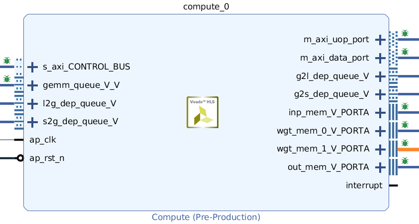
What I want to do is to check how many load and compute operation are overlapped in actual hardware. (I’m using VTA ported on ZCU104 thanks to update version pynq v0.0.1)
However, I encountered two problem.
First, it was difficult for me to understand how the C code translates into the module as shown in the picture.
Second, the way to measure the overlapped cycles between load module and compute module.
Oh, I recently started working on vta, and currently I’m trying to see the overlapped cycles also, just like you said above.
Can you give me some advises?
Where can I find the generated code from C->verilog code of vta?
Which part do I have to focus on, to see the parts, where the cycles are fused together?
Thanks in advance
Moreover, I’m trying to find how the vta works inside PYNQ board, how the code generates verilog bitstream file and make the VDLA work.
I suppose you went there much earlier, so a little help would really be great help for me!!
And I think you are perfectly right that I should try harder by myself
One thing, about the overlapping, why I started trying look for it was because on the debugged instructions,
I could see the instruction stream and how many instructions were given on one project,
but I wanted to see how the actual flow is run inside pynq cuz actually those instructions will be overlapped in some ways which are not there on the debugger like the picture below
I started with checking out if my code actually works in FPGA.
Because, until yesterday I did not ‘make’ the makefile of tvm/vta/hardware/xilinx, which means I did not have the bit file.
I just realized that if I don’t have the bit file, tvm just takes the default one from github.
While doing this, I got a question if you know the answer.
If I start vivado project, the project of pynq is based on xc7z020clg484-1, which should actually be 400 as the board says.
I connected the output signal that controls each modules(load, store, compute, gemm) to 4 leds and checked out that they(the control signals) are given but, I had to change the Project part to xc7z020clg400 to set the led output. And it works fine except, could not finish the work.
In other words, the last instruction which is FINISH does not work and the workflow can’t come back to my host side. I had to manually turn off PYNQ board power and crash it to stop.
I thought the only change I made that caused this fault was change of project part. So I think that might have caused the problem.
Do you know why it is set to a different one from PYNQ-Z1 board FPGA?
Do you have xc7z020clg484-1 FPGA on your pynq board?
Because mine has xc7z020clg400 on my board.
Thats why I was asking.
Also thanks for your advise that I should connect LEDs when modules take data from queue,
I just AND ed the axi control signals out of PS part that controls PL part in short. Do you think that might have caused the problem? All the modules (load, store, compute, gemm) did work and I could see it by the LEDs being turned on. It’s just that FINISH work did not work well.
I’m so happy I have someone to talk about this thank you so much for replying
I am currently looking at tracing the time it takes for the data to reach the fetch, load, and compute module, Can you please support with the best approach for this?