Do we have any way to process codegen with more fine grade control?

I’m currently reading some asm code from ACL, and trying to reproduce some great design in TVM using schedule primitives, but failed to get codegen result as I expected.

For example there’re 32 vector register files in the ARMv8 Neon instruction set, each has 128 bit. By adding cache_read/cache_write and some schedule primitives, I can somehow get a schedule like this in a 510 * 512 * 512 matmul workload:

primfn(A_1: handle, B_1: handle, C_1: handle) -> ()
  attr = {"global_symbol": "main", "tir.noalias": True}
  buffers = {C: Buffer(C_2: Pointer(float32), float32, [510, 512], [], align=64),
             B: Buffer(B_2: Pointer(float32), float32, [512, 512], [], align=64),
             A: Buffer(A_2: Pointer(float32), float32, [510, 512], [], align=64)}
  buffer_map = {A_1: A, B_1: B, C_1: C} {
  attr [C.local: Pointer(float32)] "storage_scope" = "local";
  allocate(C.local, float32, [96]);
  attr [A.local: Pointer(float32)] "storage_scope" = "local";
  allocate(A.local, float32, [24]);
  attr [B.local: Pointer(float32)] "storage_scope" = "local";
  allocate(B.local, float32, [8]);
  for (i.outer: int32, 0, 85) {
    for (j.outer: int32, 0, 32) {
      for (j.c.outer.outer.inner.init: int32, 0, 2) {
        for (i.c.inner.init: int32, 0, 6) {
          for (j.c.outer.inner.init: int32, 0, 2) {
            C.local[ramp((((i.c.inner.init*16) + (j.c.outer.outer.inner.init*8)) + (j.c.outer.inner.init*4)), 1, 4)] = broadcast(0f32, 4)
          }
        }
      }
      for (k.outer: int32, 0, 128) {
        for (ax0: int32, 0, 6) {
          A.local[ramp((ax0*4), 1, 4)] = (float32x4*)A_2[ramp((((i.outer*3072) + (ax0*512)) + (k.outer*4)), 1, 4)]
        }
        for (j.c.outer.outer.inner: int32, 0, 2) {
          for (k.inner: int32, 0, 4) {
            B.local[ramp(0, 1, 8)] = (float32x8*)B_2[ramp(((((k.outer*2048) + (k.inner*512)) + (j.outer*16)) + (j.c.outer.outer.inner*8)), 1, 8)]
            for (i.c.inner: int32, 0, 6) {
              for (j.c.outer.inner: int32, 0, 2) {
                C.local[ramp((((i.c.inner*16) + (j.c.outer.outer.inner*8)) + (j.c.outer.inner*4)), 1, 4)] = ((float32x4*)C.local[ramp((((i.c.inner*16) + (j.c.outer.outer.inner*8)) + (j.c.outer.inner*4)), 1, 4)] + (broadcast((float32*)A.local[((i.c.inner*4) + k.inner)], 4)*(float32x4*)B.local[ramp((j.c.outer.inner*4), 1, 4)]))
              }
            }
          }
        }
      }
      for (i.inner: int32, 0, 6) {
        C_2[ramp((((i.outer*3072) + (i.inner*512)) + (j.outer*16)), 1, 16)] = (float32x16*)C.local[ramp((i.inner*16), 1, 16)]
      }
    }
  }
}

I was willing to get a final codegen result with C.local assigned 24 register files, A.local assigned 6 register files and B.local assigned 2 register files. While the asm result of llvm is totally different from what I expected.

Emm … I know it seems difficult to reproduce an asm design after multiple level’s conversion(TE schedule primitives → IR AST → LLVM → ASM code), but still want to know if there is any possibility to control it better.

Will the new TIR more likely to be “what you see is what you get” compared to the original TE?

(p.s. Is “local” memory scopy guaranteed to generate a memory buffer in register?)

cc @tqchen @FrozenGene @junrushao

also cc @giuseros who might have more insights into ARM

We have similar observation that LLVM is unable to produce what we exactly want when it comes to very low-level control (e.g. registers, pipeline depth, etc). A way to obtain fine-grained control is to embed TVM intrinsics that could be lowered to ASM.

BTW, if you would like to play around with TIR, you might be interested in the new round-trippable TVM script that @spectrometerHBH and @Hzfengsy developed (API: tvm.script.asscript, tvm.script.tir). We can actually print out the IR, manually manipulate it, then parse it back. It means that we don’t need to be limited by those existing schedule primitives, but can control the TIR at any stage of those passes.

When we want to do some advanced optimization like register blocking the goal you want to achieve , TVM codegen can not handle it very well. My experience is 1. write micro gemm like 4x4 or 8x8 and then tensorize 2. try, try and try different schedule and find one combination to match your expectation, it is very painful. Maybe tensorir like @junrushao mentioned could solve it better, but I don’t think it could solve this low level fine-grained control problem completely.

1 Like

@junrushao Yeah I see, but seems we’re not yet able to lower & build a TIR module in the master branch now? :laughing: (Maybe I can have a try on the tensorir private branch…)
@FrozenGene I agree, I think this is the limitation of all the high level abstractions, other implementation may in the end have a same problem. So looks like it will be more difficult to achieve our goal of using techniques like Ansor to solve most of the performance problem in different devices…

Another investigation is that there’s a code snippet in ACL like:

      ......
      "ldr q6, [x15, #0x0]\n"
      "fmla v8.4s, v6.4s, v0.s[0]\n"
      ......
      "ldr q6, [x15, #0x40]\n"
      "fmla v8.4s, v6.4s, v0.s[1]\n"
      ......
      "ldr q6, [x15, #0x80]\n"
      "fmla v8.4s, v6.4s, v0.s[2]\n"
      ......
      "ldr q6, [x15, #0xc0]\n"
      "fmla v8.4s, v6.4s, v0.s[3]\n"
      ......

Which produces the SIMD fma across the data loaded to (q6/v6) and the data stored in v0.

But the asm generated by TVM seems to never use buffer like v*.s[1], v*.s[2], v*.s[3]. I think this is a simpler problem than the register buffer control.

1 Like

The parser and printer is ready on mainline and supports manipulating either TensorIR or low-level TIR. @vinx13 is playing with it right now on GPU codegen.

The TensorIR lowering process is not yet fully on mainline, but let’s expect it very soon. @Hzfengsy is almost ready to submit a PR.

As @FrozenGene mentioned, it is really challenging when it comes to low-level codegen, and i totally agree with the 4x4/8x8 microkernel approach.

1 Like

Yeah, it is unfriendly for Ansor. However, I think it is not contradict. We could not expect we could generate asm like ACL, but we could expect we could achieve the same optimization. For example, your example is we can not do register blocking optimization easily, but we could expect we have done FMA optimization like ACL, so we generate fmla correctly too. For the CPU part, in my opinion, even we can not generate the same asm snippet, but we maybe could get the same level of performance if we could generate key instruction like fmla. If we can not, there must be one factor we ignore, maybe memory access unfriendly so that we have high rate of cache miss or what else.

back to ansor, we of course should improve our ansor’s performance, however, for the most performance gemm micro part, I think the most practical way in the current time, is we should leverage micro gemm kernel (4x4/8x8) and let ansor or metaschedule to schedule other part (like tiling parameter / unroll / parallel or what else)

2 Likes

All we need is a target backend which can emit and optimize intrinsic ir.

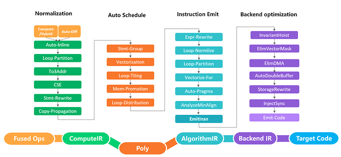
Let’s take a look at what we’ve done in akg, which is a tensor compiler for Davinci core based on tvm.

Why we do this?

  1. NPU has more SIMD intrinsics than GPU/ARM, but we can not count on LLVM for auto vectorization/tensorzation,
  2. So low level LLVM compiler provides a c/c++ & intrinsic languages for users,
  3. But c/c++ & intrinsics is very unfriendly to program, First users need to learn lots of things related to ISA and target machine, Sencond, LLVM always treate intrinsics as black boxes, which means users have to optimize code manualy.
  4. Besides, NPU SIMD is more complicated and flexible than tradditinal SIMD. NPU SIMD can support move/compute data with mutliple strides, with it you may move blocks each instruction. For the same loop nests, we may have different configurations when we map it into intrinsics, and different configurations means different performance on NPU. It’s a big burden for users when they use c/c++ & intrinsics directly.
  5. also we can do lots of target related optimization here, see them in graph above.

For @jcf94 's issue, basically it’s the same with ours, except intrinsics of ARM/RISCV is much simplier than NPU(just one dimension SIMD). If we want to control more details, we should support emiting and optimzing intrinsics in TIR. Which means we may have target backends in TIR. If just support normal cpu/gpu target, it is enough.

3 Likes

I post an exmple for intrinsics choosing.

for (i, 0, 65535) {
   C[i] = (A[i] + B[i])
}
Call Engine: veadd_mm
// normal ===stmt cost : 2061.94 (smallest cost) shape : 1x65535
 [ tx.veadd_mm(tir.tvm_access_ptr(tir.type_annotation(), C, (int64)0, (int64)65535, 2), tir.tvm_access_ptr(tir.type_annotation(), A, (int64)0, (int64)65535, 1), tir.tvm_access_ptr(tir.type_annotation(), B, (int64)0, (int64)65535, 1), tx.csrw("CSR_SHAPE_S1_COL", (int64)65535, "CSR_SHAPE_S1_ROW", (int64)1, "CSR_STRIDE_D", (int64)0, "CSR_STRIDE_S", (int64)0))
 ]

// normal and align === stmt cost : 2071.91 shape : 1x65472 
 [ tx.veadd_mm(tir.tvm_access_ptr(tir.type_annotation(), C, (int64)0, (int64)65535, 2), tir.tvm_access_ptr(tir.type_annotation(), A, (int64)0, (int64)65535, 1), tir.tvm_access_ptr(tir.type_annotation(), B, (int64)0, (int64)65535, 1), tx.csrw("CSR_SHAPE_S1_COL", (int64)65472, "CSR_SHAPE_S1_ROW", (int64)1, "CSR_STRIDE_D", (int64)0, "CSR_STRIDE_S", (int64)0))
tx.veadd_mm(tir.tvm_access_ptr(tir.type_annotation(), C, (int64)65472, (int64)63, 2), tir.tvm_access_ptr(tir.type_annotation(), A, (int64)65472, (int64)63, 1), tir.tvm_access_ptr(tir.type_annotation(), B, (int64)65472, (int64)63, 1), tx.csrw("CSR_SHAPE_S1_COL", (int64)63, "CSR_SHAPE_S1_ROW", (int64)1, "CSR_STRIDE_D", (int64)0, "CSR_STRIDE_S", (int64)0))
 ]

// reshape === stmt cost : 131080
 [ tx.veadd_mm(tir.tvm_access_ptr(tir.type_annotation(), C, (int64)0, (int64)65535, 2), tir.tvm_access_ptr(tir.type_annotation(), A, (int64)0, (int64)65535, 1), tir.tvm_access_ptr(tir.type_annotation(), B, (int64)0, (int64)65535, 1), tx.csrw("CSR_SHAPE_S1_COL", (int64)1, "CSR_SHAPE_S1_ROW", (int64)65535, "CSR_STRIDE_D", 0, "CSR_STRIDE_S", 0))
 ]

// === stmt cost : 786420 
 [ for (i, 0, (int64)65535) {
  tx.veadd_mm(tir.tvm_access_ptr(tir.type_annotation(), C, int64(i), ((int64)65535 - int64(i)), 2), tir.tvm_access_ptr(tir.type_annotation(), A, int64(i), ((int64)65535 - int64(i)), 1), tir.tvm_access_ptr(tir.type_annotation(), B, int64(i), ((int64)65535 - int64(i)), 1), tx.csrw("CSR_SHAPE_S1_COL", (int64)1, "CSR_SHAPE_S1_ROW", (int64)1, "CSR_STRIDE_D", (int64)0, "CSR_STRIDE_S", (int64)0))
}
 ]

Call Engine: veadd_mv_dimh
// normal === stmt cost : 3085.91
 [ tx.veadd_mv_dimh(tir.tvm_access_ptr(tir.type_annotation(), C, (int64)0, (int64)65535, 2), tir.tvm_access_ptr(tir.type_annotation(), B, (int64)0, (int64)65535, 1), tir.tvm_access_ptr(tir.type_annotation(), A, (int64)0, (int64)65535, 1), tx.csrw("CSR_SHAPE_S1_COL", (int64)65535, "CSR_SHAPE_S1_ROW", (int64)1, "CSR_STRIDE_D", (int64)0, "CSR_STRIDE_S", (int64)0))
 ]

// normal and align === stmt cost : 2069.94
 [ tx.veadd_mv_dimh(tir.tvm_access_ptr(tir.type_annotation(), C, (int64)0, (int64)65535, 2), tir.tvm_access_ptr(tir.type_annotation(), B, (int64)0, (int64)65535, 1), tir.tvm_access_ptr(tir.type_annotation(), A, (int64)0, (int64)65535, 1), tx.csrw("CSR_SHAPE_S1_COL", (int64)65472, "CSR_SHAPE_S1_ROW", (int64)1, "CSR_STRIDE_D", (int64)0, "CSR_STRIDE_S", (int64)0))
tx.veadd_mv_dimh(tir.tvm_access_ptr(tir.type_annotation(), C, (int64)65472, (int64)63, 2), tir.tvm_access_ptr(tir.type_annotation(), B, (int64)65472, (int64)63, 1), tir.tvm_access_ptr(tir.type_annotation(), A, (int64)65472, (int64)63, 1), tx.csrw("CSR_SHAPE_S1_COL", (int64)63, "CSR_SHAPE_S1_ROW", (int64)1, "CSR_STRIDE_D", (int64)0, "CSR_STRIDE_S", (int64)0))
 ]

// === stmt cost : 720885
 [ for (i, 0, (int64)65535) {
  tx.veadd_mv_dimh(tir.tvm_access_ptr(tir.type_annotation(), C, int64(i), ((int64)65535 - int64(i)), 2), tir.tvm_access_ptr(tir.type_annotation(), B, int64(i), ((int64)65535 - int64(i)), 1), tir.tvm_access_ptr(tir.type_annotation(), A, int64(i), ((int64)65535 - int64(i)), 1), tx.csrw("CSR_SHAPE_S1_COL", (int64)1, "CSR_SHAPE_S1_ROW", (int64)1, "CSR_STRIDE_D", (int64)0, "CSR_STRIDE_S", (int64)0))
}
 ]
Call Engine: veadd_mf
// === stmt cost : 720885
 [ for (i, 0, (int64)65535) {
  tx.veadd_mf(tir.tvm_access_ptr(tir.type_annotation(), C, int64(i), ((int64)65535 - int64(i)), 2), tir.tvm_access_ptr(tir.type_annotation(), B, int64(i), ((int64)65535 - int64(i)), 1), A[i], tx.csrw("CSR_SHAPE_S1_COL", (int64)1, "CSR_SHAPE_S1_ROW", (int64)1, "CSR_STRIDE_D", (int64)0, "CSR_STRIDE_S", (int64)0))
}
 ]

So we need a big module(lots of design and code) to emit intrinsics, tensorization at the first place doesn’t fit well for NPUs.